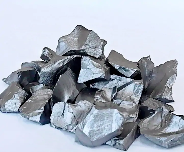
Разновидность элементарного кремния с серым металлическим блеском, широко используемая в фотоэлектрической промышленности и производстве интегральных микросхем.
Polysilicon is mainly used in the photovoltaic and integrated circuit chip fields. In the photovoltaic field, it is the core material of the upstream industrial chain of photovoltaic solar panels; in the integrated circuit chip field, it serves as a chip substrate to support the production of precision electronic devices. It is typically produced by the Modified Siemens method, a mainstream technology that obtains rod-shaped polysilicon through the reduction deposition of trichlorosilane (SiHCl₃).
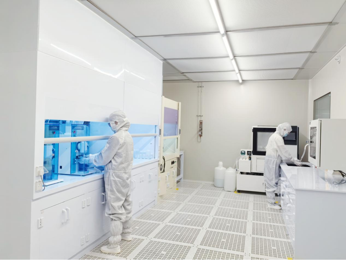
ISO Class 5, 6, and 7 clean workshops, precise control, and real-time monitoring.
Quality meets customer needs, and the standard exceeds the quality requirements of N-type cells.
| Product Name | Appearance and size requirements |
| Re-feeding | Polysilicon has no color spots, discoloration, visible pollutants, interlayers and holes: linear size 8mm-50mm. No more than 5% of each bag is less than 8mm and greater than 50mm; no more than 0.10% is less than 3mm; no more than 15% of the cauliflower with a linear gap depth of 5-20mm; it does not include silicon core detached silicon material and silicon material within 150mm from the carbon head, and silicon core discoloration or peeling is strictly prohibited. |
| Coral | Block polysilicon, no color spots, discoloration, no visible contaminants, interlayers and silicon core holes: linear size 8mm-50mm; less than 3mm not more than 0.10%, linear gap depth greater than 20mm. Silicon core discoloration or peeling is strictly prohibited. |
| Crushed | No color spots, no visible pollutants, no oxidation interlayers, linear dimensions controlled within 3mm-8mm. Less than 3mm does not exceed 0.3% (of which less than 1mm does not exceed 0.1%); no distinction is made between dense, cauliflower, and coral. |
| Small scraps | No color spots, no visible pollutants, no oxide interlayers, linear dimensions controlled within 1mm-3mm. No more than 5% are smaller than 1mm (and no more than 0.1% are smaller than 0.5mm). |
| Electronic Premium | Electronics Ⅰ | Electronics Ⅱ | Electronics Ⅲ | Solar Premium | |
| Donor impurity content (total content of P, As, Sb) ppba | ≤0.03 | ≤0.05 | ≤0.10 | ≤0.30 | ≤0.68 |
| Acceptor impurity content (total content of B and Al) ppba | ≤0.01 | ≤0.03 | ≤0.05 | ≤0.10 | ≤0.26 |
| Carbon concentration/ppma | ≤0.02 | ≤0.05 | ≤0.05 | ≤0.10 | ≤4 |
| Matrix metal impurity content (total content of Fe, Cr, Ni, Cu, Zn, Na) ng/g (ppbw) | ≤0.1 | ≤0.3 | ≤0.5 | ≤2.0 | ≤15 |
| Surface metal impurity content (total content of Fe, Cr, Ni, Cu, Zn, Al, K, Na, Ti, Mo, W, Co) ng/g (ppbw) | ≤0.1 | ≤0.5 | ≤1.0 | ≤5.0 | ≤30 |
Note: The conductivity type, resistivity, minority carrier lifetime and oxygen content of polysilicon are determined by negotiation between the supplier and the buyer.
50,000 tons per year
CSG has an ISO Class 5 clean laboratory equipped with world-class testing instruments, including ICP-MS, ICP-OES, LTFT-IR, GC-MS, GC, FZ, an automatic potentiometric titrator, a high-frequency infrared carbon and sulfur analyzer, 1/10,000 and 1/100,000 precision balances, and more.

Test1