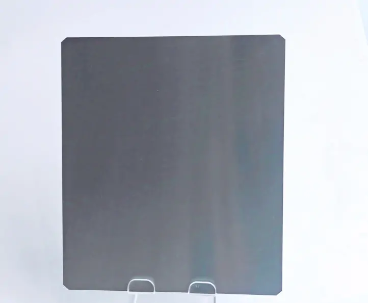
CSG’s monocrystalline silicon wafers are produced from high-purity silicon using the CZ (Czochralski) method. The standard thickness ranges from 130 to 150 μm, with diameters between 182 mm and 210 mm. These wafers feature high photoelectric conversion efficiency and low degradation. They are specifically used as the core substrate of high-efficiency photovoltaic cells and serve as a fundamental material in the clean energy industry chain.